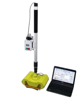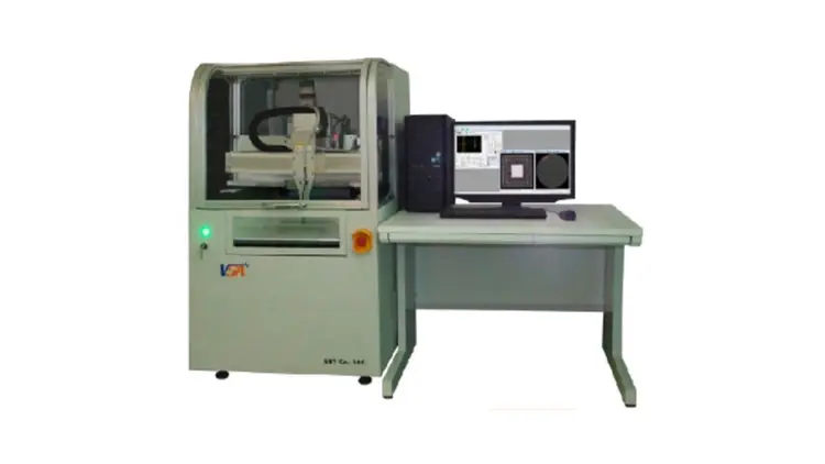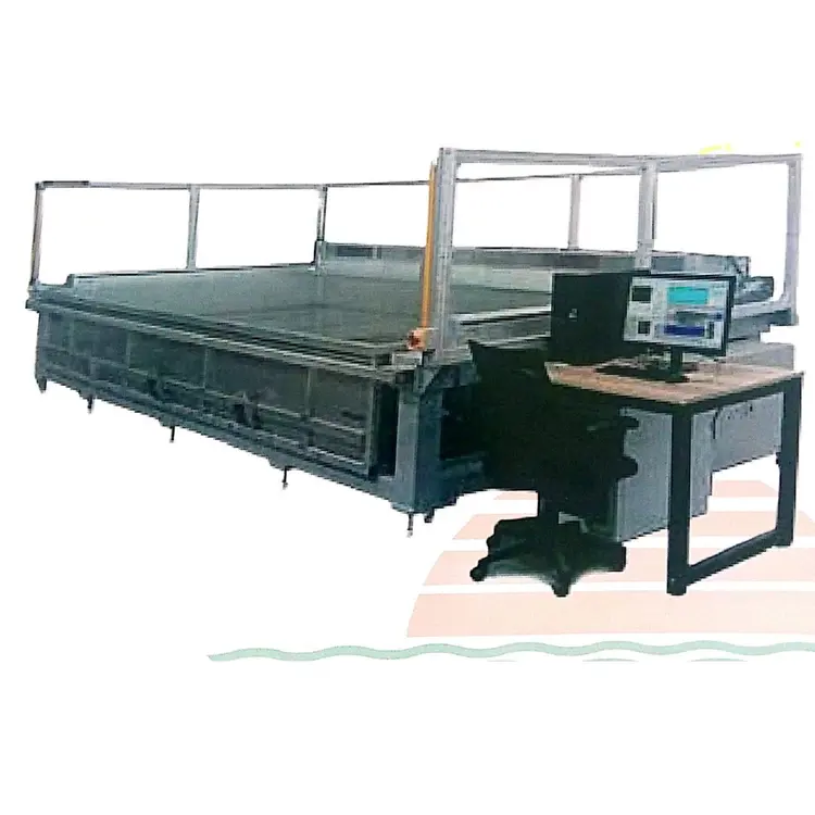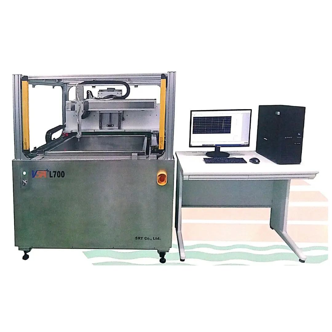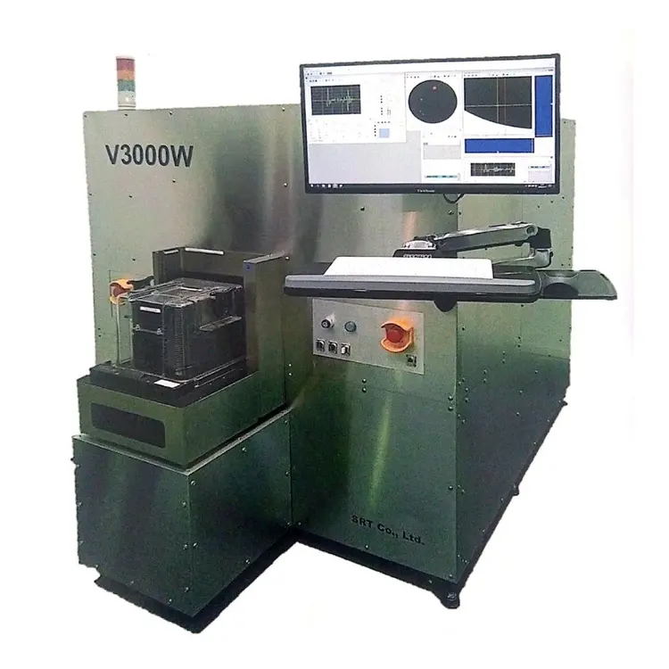
Ultrasound Imaging Device V3000W
| Manufacturer | SRT Co. Ltd. |
| Product Code | . |
| Product HSN Code | |
| Shipping | Shipped in 6 to 8 weeks |
| Stock Availability | Available On Demand |
PRODUCT DESCRIPTION / OVERVIEW
Advantage of the Ultrasound Imaging Device V3000W:
- The V3000W ultrasound imaging device is designed for high-resolution inspection across various industrial applications. With advanced imaging technology, this device ensures precise flaw detection and material evaluation. The lightweight and compact design makes it ideal for portable operations, while the user-friendly interface allows for quick setup and seamless data interpretation.
ABOUT THE PRODUCT
| Country of Origin: | Japan | |||
| Industry the product belogs to: |
| |||
| Application of the product: | Automation and Control | |||
| Supplier location: | Navi Mumbai |
PRODUCT SPECIFICATIONS
| Wafer Size (X × Y): | 12 |
| Scan Speed: | 1200 mm/s |
| Resolution: | 0.001 mm |
| Power Supply: | AC 200–220 V, 20 A |
| Body Size (W × D × H): | 1500 × 1480 × 1550 mm |
| Weight: | 850 kg |
| Interlock: | Emergency Button, Door Sensor |
| Inspect Mode: | C-Scan, Program-scan, Warpage-scan, Index-scan, Full Waveform Scan |
| Analyze Method: | Defect Area Measurement, Defect Position Measurement, Color Thresholding, Waveform Analysis, Image Processing by FFT |
| Options: | Water Filter Unit, Ultrasonic Sensor (5–150 MHz), Sensor Adapter |
FAQs
The V3000-W Ultrasound Imaging Device is a non-destructive testing (NDT) system designed for ultrasonic inspection of 6-inch to 12-inch semiconductor wafers. It detects internal defects such as voids, delamination, cracks, and bonding issues while ensuring high-speed, accurate quality inspection.
The V3000-W is widely used in semiconductor manufacturing, electronics production, wafer fabrication facilities, quality control laboratories, research institutions, and advanced industrial inspection applications requiring precise ultrasonic imaging.
Key features include support for 6-inch to 12-inch wafer cassettes, high-speed scanning up to 1200 mm/s, automated defect analysis using area and area ratio calculations, network-based inspection result management, and an all-stainless-steel scanner for reliable industrial operation.
The V3000-W detects internal defects such as delamination, voids, cracks, bonding failures, and other structural imperfections in semiconductor wafers. Its high-resolution ultrasonic imaging helps improve product quality and manufacturing reliability.
Yes, the V3000-W is designed for inline semiconductor manufacturing and can be customized to meet production line requirements. It supports automated inspection workflows, host computer connectivity, and application-specific configurations for enhanced inspection efficiency.