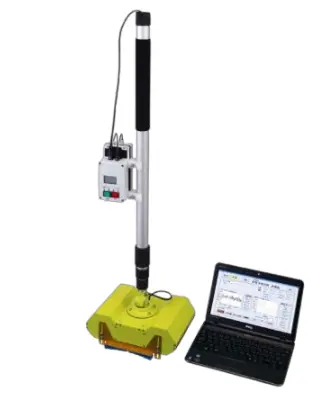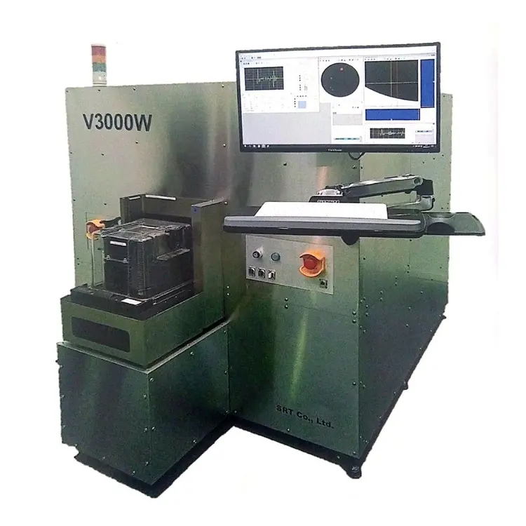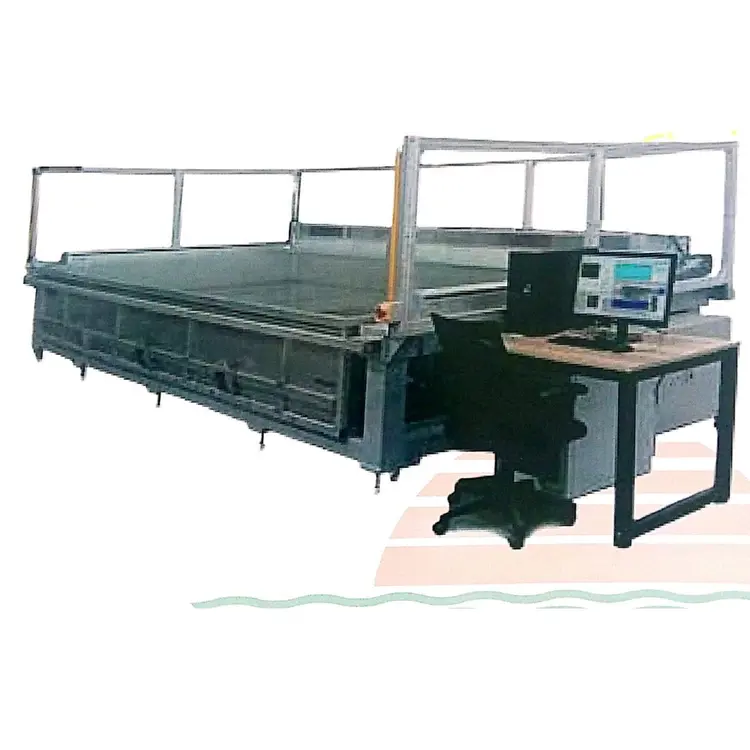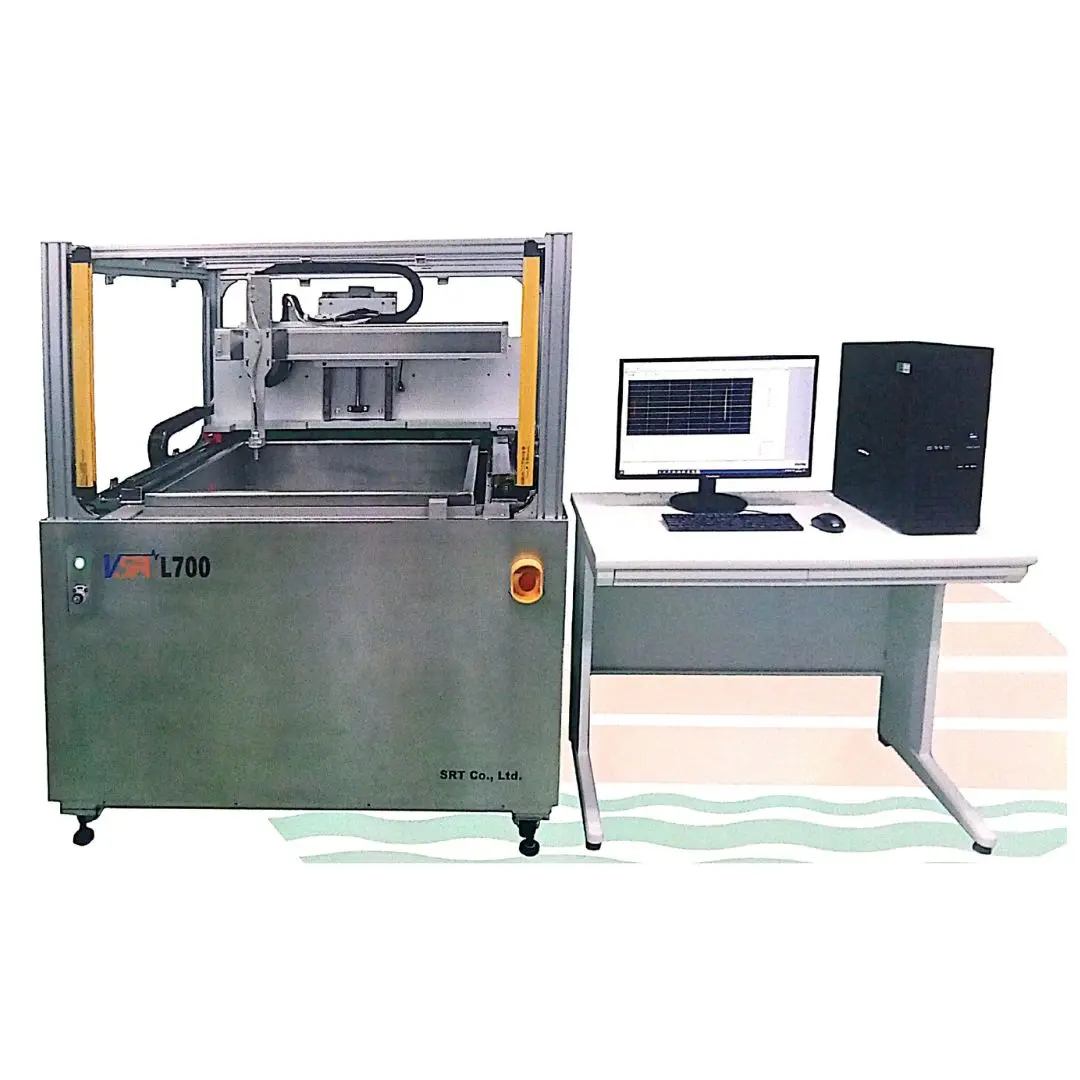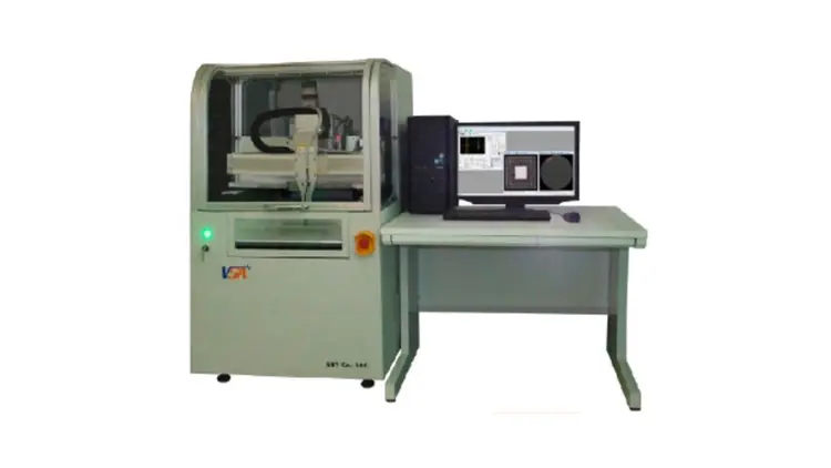
Ultrasound Imaging Device VSA M-350
| Manufacturer | SRT Co. Ltd. |
| Product Code | . |
| Product HSN Code | |
| Shipping | Shipped in 7 - 8 weeks |
| Stock Availability | Available On Demand |
PRODUCT DESCRIPTION / OVERVIEW
Advantage of the Ultrasound Imaging Device VSA M-350:
- This is an ultrasonic imaging device that uses Scanning Acoustic Tomography (SAT) to analyze Integrated Circuit (IC) failures. It is a compact, stable, and user-friendly machine. It has a standard calibration function that enables it to keep in focus any time reproduction of an image takes place, as well as an auto-calibration feature. It is easy to set parameters. It supports mass inspection with programmable scanning techniques for automatic flaw analysis and center adjustment. The defective IC chips are rejected/sorted by robotic arm. The high-resolution imaging allows flexible layouts for displaying inspection results.
ABOUT THE PRODUCT
| Country of Origin: | Japan | |||
| Industry the product belogs to: |
| |||
| Application of the product: | Automation and Control | |||
| Supplier location: | Navi Mumbai |
PRODUCT SPECIFICATIONS
| Scan Range (XYZ): | 350 × 320 × 80 mm |
| Scan Speed: | 1200 mm/s |
| Measurement Pitch: | 0.001 mm |
| AC Power Supply: | 100 V/200 V, 15 A |
| Supply Body Size (W × D × H): | 780 × 900 × 1250 mm |
| Quantity: | About 350 kg |
| Safety Devices: | Emergency Stop Button, Door Open/Close Detection Sensor |
| Available Measurement Mode: | C-Scan, Tray-scan, Through-scan, Index-scan, Grid-Scan, Full Waveform Scan |
| Analysis Function: | 1. Defect Area Measurement; 2. Defect Location Measurement; 3. Defect Binary Display; 4. Waveform Analysis; 5. FFT Video Processing Probe Option |
FAQs
The VSA M350 Ultrasound Imaging Device is a high-precision non-destructive testing (NDT) system designed for inspecting IC packages, 300 mm wafers, MLCCs, JEDEC trays, and automotive electronic components. It detects internal defects such as voids, delamination, cracks, and bonding failures without damaging the test sample.
The VSA M350 is widely used in semiconductor manufacturing, electronics production, automotive electronics, PCB assembly, research laboratories, and quality inspection facilities for advanced ultrasonic imaging and internal defect analysis.
Key features include a 350 × 350 × 80 mm scanning area, 100 million-pixel ultrasonic imaging, up to 1200 mm/s scanning speed, 0.001 mm measurement pitch, a standard 35 MHz probe, and support for multiple inspection modes, including C-Scan, Through-Scan, Grid-Scan, and Full Waveform Scan.
The VSA M350 accurately detects internal defects such as delamination, voids, cracks, poor solder joints, bonding failures, and other structural imperfections in semiconductor devices, wafers, MLCCs, and electronic components, ensuring reliable quality control and failure analysis.
Yes, the VSA M350 supports multiple probe frequencies ranging from 5 MHz to 150 MHz and offers optional transmission measurement, multi-probe erosion measurement, and application-specific fixtures, making it suitable for a wide range of semiconductor and industrial inspection requirements.